Kyocera has announced its plans to commence construction of a new research and development centre at its Kokubu campus in Kirishima City, Kagoshima, Japan, in January 2021.
A location agreement has been signed by the company with the mayor of Kirishima City for the new R&D centre.
Go deeper with GlobalData

Discover B2B Marketing That Performs
Combine business intelligence and editorial excellence to reach engaged professionals across 36 leading media platforms.
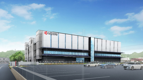
This $96m centre will focus its research and development activities on information and communications, environmental preservation, and smart energy.
The Kokubu campus already serves as a site for three R&D groups: Monozukuri R&D Laboratory, Production Technology Division, and Analysis Center
Currently, the research and development programmes undertaken at the campus include on electronic and semiconductor components used in IoT devices, 5G smartphone technologies, and important components for smart energy technologies, such as cell stacks for Solid Oxide Fuel.
The centre will be a five-storey steel construction, with 22,902m2 of floor space. It is expected to open by September 2022.

US Tariffs are shifting - will you react or anticipate?
Don’t let policy changes catch you off guard. Stay proactive with real-time data and expert analysis.
By GlobalDataKyocera plans to set up a new platform to speed up development and production efforts, with support for manufacturing new products, promotion of factory automation, and bolstering production efficiencies.
The centre will focus on development of laminated ceramic capacitors, ceramic packages for electronic devices, cell stacks for SOFCs.
It plans to position the new facility as an incubator for open innovation. This facility will enable in sharing of technical information for human resource development, as well as networking with inventors outside of the firm.
————————————————————————————————————————————
Architect’s rendering of the new R&D centre. (Centre: Business Wire)